Friday, September 19, 2014
Homebrew DCF 77 Signal Generator

The DCF77 signal is a long-wave time signal transmitted from Mainflingen, Germany, providing highly accurate time synchronization across Europe. This signal is used in clocks, timers, and devices requiring precise timekeeping. Building a homebrew DCF77 signal generator allows hobbyists to experiment with time synchronization for clocks or even emulate a DCF77 signal in areas without reception.
This article outlines how to create your own DCF77 signal generator using basic electronic components and microcontroller programming.
Understanding DCF77 Signals
The DCF77 signal carries both time and date information. It is transmitted on a 77.5 kHz carrier wave modulated by amplitude. Each minute, 59 bits of information are transmitted:
- Seconds 0-20: Reserved for status information.
- Seconds 21-58: Encodes time, date, and parity bits.
- Second 59: A blank bit (no signal) indicates the end of a minute.
The signal uses pulse-width modulation:
- A short pulse (100 ms) represents a binary 0.
- A long pulse (200 ms) represents a binary 1.
Components Required
To build a DCF77 signal generator, you will need:
- Microcontroller: Arduino or ESP32 is recommended for flexibility.
- Crystal Oscillator: For generating a stable 77.5 kHz carrier wave.
- Transistors/MOSFETs: For signal amplification.
- Resistors and Capacitors: For signal conditioning.
- Breadboard/PCB: For prototyping the circuit.
- Coil Antenna: To simulate the DCF77 signal wirelessly (optional).
- Power Supply: Suitable for your microcontroller and additional components.
Circuit Design
The DCF77 generator can be broken into three stages:
1. Carrier Wave Generation
Generate a stable 77.5 kHz sine or square wave using the microcontroller. Alternatively, use a crystal oscillator to produce the frequency directly.
2. Amplitude Modulation
Use the microcontroller to modulate the carrier wave based on the DCF77 data bits. This involves toggling between a high and low amplitude to encode the signal.
3. Signal Transmission
Optionally amplify and transmit the signal through a coil antenna to nearby receivers. If using a wired connection, output the modulated signal directly.
Programming the Microcontroller
A microcontroller such as Arduino can handle signal modulation. Below is an example sketch for Arduino:
This program generates a 77.5 kHz carrier wave and modulates it based on DCF77 timing. You can customize the timing to match the official signal encoding.
Testing the Signal
- Use an oscilloscope to verify the carrier frequency and amplitude modulation.
- Place a DCF77-compatible clock nearby to test if it syncs with the signal.
- Experiment with signal strength and antenna placement for optimal results.
Applications
- Clock Calibration: Synchronize clocks in areas without DCF77 reception.
- Educational Tool: Learn about signal generation and timekeeping protocols.
- Custom Time Servers: Integrate with IoT devices needing precise time.
Conclusion
Building a homebrew DCF77 signal generator is an engaging project combining electronics, programming, and physics. With minimal components and basic programming, you can simulate a highly accurate time signal. Whether for educational purposes or practical applications, this project is a rewarding addition to any DIY electronics portfolio.

Tuesday, February 4, 2014
Car 12V to 50V DC Converter Circuit Diagram

This circuit for Car audio input battery 12V to 50VDC, It use transistor and IC TL072.
Saturday, January 11, 2014
cell phone jammer is to shield the GSM frequency band
band, CDMA frequency band and 3G frequency band at the same time.
And broadcasting 24 hours. Fourth, the development prospects of Chinas mobile TV and countermeasures of Chinas mobile TV prospects for the development and Countermeasures 4.1 bottlenecks in the
development of mobile TV to the diverse needs of the audience on the mobile terminal is gradually increasing, making the mobile TV market has shown signs of the trend gaining momentum, the future
can not Limited. Country in the process of development of mobile TV, in some respects, has achieved some success, but also suffered a number of bottlenecks, such as regulatory policy confusion,
lack of communication content, communication technology is lagging behind the lack of professional mobile TV professionals, the use of tariff The high technical standards are not uniform and other
bottlenecks. Regulatory policy confusion. But the area out of the shielding range will not be affected by cell phone jammer .
Management regulations in the telecommunications or radio and television and the management of the mobile TV business clearly defined, the Ministry of Industry and SARFT there mobile TV The
controversy led by whom. In order to capture this emerging mobile TV market high ground, handset manufacturers, telecom operators, radio and television operators have joined the field, the media to
be outdone involved. In accordance with the relevant provisions of the Administration of Radio, all those engaged in online audio and video programs play unit must apply to the Radio and Television
Information Network 09016475 "introduced by the end of 2000, the Telecommunications Ordinance expressly provides image transmission is also a telecommunications areas The former belongs to the
administrative provisions, while the latter is the national laws and regulations. cell phone jammer is developed and manufactured on the basis of the existing product.
The two cross-cutting policies and regulations so that the regulatory policies of the mobile TV 17 confusion. Chaotic regulatory policy also caused a conflict of interest between different
departments, can not reach a consistent understanding of the operating mode of the mobile TV standards, and not within the legal and institutional framework for effective coordination of
broadcasting and telecommunications, and rural development, therefore very make life difficult for the development of mobile TV to create a stable communication environment, hinder the development
process of mobile TV. Secondly, the chaotic regulatory policy to the mobile TV services to carry out the obstacles. For example, some wishing to launch mobile TV service company, to get the mobile
TV business license must apply to the different authorities. cell phone jammer cab be validly used in the prison, detention house, labor camp and so on.The design of cell phone jammer is totally
developed by the nation
Safe Constant Current Source Circuit Diagram

Friday, December 27, 2013
Single Supply fault Monitor Circuit Diagram

Wednesday, December 25, 2013
Environmentally Friendly Mosquito Repeller
We might mention the well-known Chinese coils – the only thing Chinese about them is undoubtedly their name – which very often drive people away as much as mosquitoes, if not more! Moreover they are nasty things to handle. There are also UV (ultra-violet) ‘electrocutors’ consisting of a blue lamp surrounded by two closely-spaced grilles between which a high voltage is applied. The mosquitoes (and fies and other flying insects) are supposedly attracted by the color of the lamp and as they approach, get electrocuted in contact with the two grilles.
The only thing you have to do is pull out the drawer from time to time and get rid of the mass of dead insects. Even though the effectiveness of these first two products remains questionable, it is less so than the one we’re nonetheless going to describe here. We’re talking about an ultrasonic mosquito repellent.
The principle, as described by its numerous promoters, is as follows. Only the female mosquitoes bite (that at least is an undisputed scientific fact) and they bite when they need to feed, and above all, to feed their eggs. In this situation, they seek to avoid the males whose ‘job’ has already been done, and so they fy away from the frequencies emitted by the males when they are on heat. This is where opinions now diverge.

According to certain publications, the frequency emitted by the male mosquitoes is said to be around 20–25 kHz, and so within the realm of ultrasound. But according to others, it is in the region of 5–7 kHz instead; frequencies that a human ear, even an elderly one, can still hear very well. Rather than spending lots of money (of the order of tens of pounds) buying such a device, which moreover generally have a fixed frequency, we’re suggesting building one yourself so that you can carry out your own research this summer, especially since the circuit proposed is very simple and cheap to build.
As the figure shows, it uses just a single IC, a CMOS type 4047. This very multi-purpose IC can be wired in very many operating modes, including that of the multivibrator or astable used here. The operating frequency is set by the external components C1, R1, and P1; the latter makes it possible to slightly adjust the frequency, given the uncertainty that exists over the most efective value…To best reproduce the high frequencies produced by the generator, the output transducer used is a simple tweeter, but it must be a piezo one.
Such a tweeter behaves in fact much like a capacitor, and so doesn’t overload the CMOS IC outputs that are incapable of supplying a substantial current, as everyone knows who’s ever worked with 400 series CMOS logic. To obtain an output signal of sufficient amplitude while being powered from a single 9 V battery, this tweeter is connected between the 4047’s Q and Q outputs, making it possible to apply complementary (antiphase) signals to the tweeter so it ‘sees’ an alternating voltage of double the supply voltage.
In purely theoretical terms, this quadruples the output power available. In practice, it’s better to regard it as tripling it, but the beneft achieved by doing it this way is nonetheless very real. All that remains is for you to place the project in the middle of the patio table or beside your lounger in order to get a taste of the calm of a summer’s evening without mosquitoes bothering you acoustically or worse, biting. At any rate, that’s what we wish for you…
Elektor Electronics 2008
Tuesday, December 24, 2013
Simple Voltage Multiplier Circuit Diagram

Saturday, December 21, 2013
Simple LED Torch
A common problem with small torches is the short life-span both of the batteries and the bulb. The average incandescent torch, for instance, consumes around 2 Watts. The LED Torch in Fig. 1 consumes just 24 mW, giving it more than 80 times longer service from 4 AA alkaline batteries (that is, up to one months continuous service). Although the torchs light output is modest, it is nonetheless quite sufficient to illuminate a pathway for walking.
Circuit Diagram :

Fig. 1 : Simple LED Torch Circuit Diagram
The LED Torch is based on a 7555 timer running in astable mode (do not use an ordinary 555). A white LED (Maplin order code NR73) produces 400 mcd light output, which, when focussed, can illuminate objects at 30 metres. Try Conrad Electronic for what appears to be a stronger white LED (order code 15 37 45-11). A convex lens with short focal length is placed in front of the LED to focus the beam. If banding occurs at the beams perimeter, use another very short focal length lens directly in front of the LED to smooth the beam.
If a different supply voltage is preferred, the value of resistor R3 is modified as follows:
9V - 470 Ohm
12V - 560 Ohm
See my "Wind-up Torch" feature article in the October 2000 edition of Everyday Practical Electronics for a completely battery-free go-everywhere torch.
Thursday, December 19, 2013
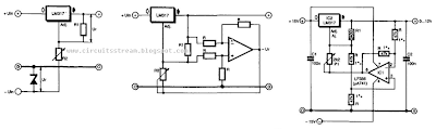
Simple But best Regulator Circuit Diagram
Tuesday, December 17, 2013
Watch Dog For Telephones
This little circuit keeps continuous watch over the telephone lines and sounds an alarm in case of any misuse. In addition it transmits a loud tone through the telephone lines to prevent further misuse. When switch S1 is turned on, the normal (on-hook) telephone line voltage at the output of bridge-rectifier diodes D1 to D4 is approximately 48 volts, which being well above the break-down voltage of zener diode D5, the diode conducts.

As a result transistor T2 gets forward biased. This effectively grounds the base of transistor T1 which is thus cut off and the remaining circuit does not get any power supply. In this state, only a small (negligible) current is taken by the circuit, which will not affect the telephone line condition. However, when handset of any telephone connected to the telephone lines is lifted (off-hook), line voltage suddenly drops to about 10 volts.
As a result, transistor T2 is switched off and transistor T1 gets forward biased via resistor R1. Now, the astable multivibrator built around timer IC1 starts oscillating and the speaker starts sounding. Output of the astable multivibrator is also connected to the base of transistor T1 through capacitor C5. As a result, only a loud (and irritating) tone is heard in the ear-piece of the unauthorized telephone instrument.
This circuit can be constructed on a veroboard using easily available low-cost components and it can be connected to any telephone line without the fear of malfunctioning. No extra power supply is required as it draws power from the telephone line for operation.
Note:
- Please disconnect the gadget when you are yourself using the telephone as it cannot distinguish between authorized and unauthorized operation.
Tuesday, October 8, 2013
Simple Transistor Tester
This is a simple circuit but we hope it will help you a lot and save your valuable time. You do not have to use millimeter to test a transistor if you build this circuit. You can have a 9 volts battery to operate the circuit. No matter if the transistor is NPN or PNP, if the transistor is shorted then no any LED should light. If the transistor is open Both the LED should light.
Now remember when you test a good PNP transistor then LED2 should light.
For NPN good transistor only LED1 should light.
Try to make the circuit on a PCB and put in a small box for its safety. Find a three pin socket and mounted it on the box. When you fix everything, only visible parts from the out side of the box should be the switch and three pins of the socket to test a transistor.

Sunday, October 6, 2013
Suzuki Swift 1997 Electrical Wiring Diagram
 |
| Suzuki Swift 1997 Electrical Wiring Diagram |
Friday, October 4, 2013
Pan Pot
 Series resistors R7 and R12 serve to ensure that the outputs can handle capacitive loads. Coupling capacitors C3, C6, and C9, may be omitted if an offset voltage of 20–30 mV is of no consequence in the relevant application. Capacitors C2, C5, and C8, ensure that the op amps remain stable even at unity gain. Capacitors C1, C4, and C7, minimize any r.f. interference, resulting in a usable bandwidth of 2.5 Hz to 200 kHz. The performance of the circuit is of sufficiently high quality to allow the pot being incorporated in good-quality control panels. Total harmonic distortion plus noise (THD+N) at a frequency of 1 kHz and a bandwidth of 22 kHz is 0.0014%. Over the band 20 Hz to 20 kHz and a bandwidth of 80 dB, this figure is still only 0.0023%. The circuit needs a power supply of ±18 V, from which it draws a current of about 16mA.
Wednesday, October 2, 2013
USB Powered PIC Programmer

Monday, September 30, 2013
Short Wave Monitor

This receiver not only gives a good indication of the myriad of stations on offer in the short-wave band but is also an excellent tool for monitoring the state of the ionosphere. The circuit actually consists of no more than an RF and an AF amplifier. The high-frequency amplification is carried out by the IF stage of a CA3089. This IC is actually intended for FM receivers, but the FM section is not used here. The internal level detector provides a signal of sufficient strength to drive an audio amplifier directly. An LM386 was selected for this task. This IC can directly drive an 8-Ω loudspeaker or headphones without any difficulty.
The power supply voltage is 9 V. Because of the modest power consumption a 9-V battery is very suitable. In addition, the circuit will work down to a voltage of about 5.5 V, so that the battery life will be extra long. The antenna will require a little experimentation. We obtained reasonable results with a piece of wire 50 cm long. A length of wire in the range of 5 to 15 meters should provide even better results at these frequencies.
Saturday, September 28, 2013
Crossover For Subwoofer
The crossover network is intended for use when an existing audio installation is to be extended by the addition of a subwoofer. Often, this additional loudspeaker is one that has been lying around for some time. If its frequency response extends down far enough, all is well and good, but a filter is then needed to cut off any frequencies above, say, 150 Hz. Often, a subwoofer network is an active filter, but here this would necessitate an additional power supply. The present network is a passive one, designed so that the speaker signal of the existing system can be used as the input signal.
Circuit diagram:
 Crossover Circuit Diagram For Subwoofer
Since the bass information is present in both (stereo) loudspeakers, the signal for the sub woofer can simply be tapped from one of them. The network is a 1st order low-pass filter with variable input (P1) and presettable cut-off frequency (P2). The signal from the loudspeaker is applied to terminal ‘LSP’. Voltage divider R1-R2-P1 is designed for use with the output signal of an average output amplifier of around d 50 W. The crossover frequency of the network may be varied between 50 Hz and 160 Hz with P2. The values of R3, P2, and C1, are calculated on the assumption that the subwoofer amplifier to be connected to K1 has a standard input resistance of 47 kΩ.
If this figure is lower, the value of C1 will need to be increased slightly. It is advisable to open the volume of the subwoofer amplifier fully and adjust the sound level with P1. This ensures that the input of the subwoofer amplifier cannot be overloaded or damaged. Make sure that the ground of the loudspeaker signal line is linked to the ground of the subwoofer amplifier. If phase reversal is required, this is best done by reversing the wires to the subwoofer. If notwithstanding the above additional protection is desired at the input of the subwoofer amplifier, this is best effected by ‘overload protection ’ elsewhere in this site.
Author: T. Giesberts Copyright: Elektor Electronics
Thursday, September 26, 2013
Float Charger For NiMH Cells
 Diode D1 protects the circuit against reverse polarity of the power supply and protects the LM317 should the power be disconnected while it is still connected to a charged battery pack. Resistor RCL and transistor Q1 limit the maximum current in the event of a short circuit or the connection of a severely discharged battery pack. LED2 provides an indication of voltage input to the charger. LED1 and the 680O resistor provide the same function for the charger output and also provide a minimum load for the regulator when the battery pack is nearing full charge. This is necessary to keep the regulator output from drifting up and damaging the batteries. The circuit uses an external DC plugpack and is suitable for four NiMH cells rated at 2.5Ah.
 Table 1 gives alternative values for 1-10 batteries in series at peak charge currents of between 200mA to 600mA. If you are using the specified plug-pack and the TO-220 packaged LM317T, you will need a heatsink rated at 12°C/W or better for any design other than the 200mA single cell charger. A TO-3 packaged device with the correct plug-pack will be OK without a heat-sink for any of the 200mA configurations and up to four cells charging at 400mA.
Tuesday, September 24, 2013
Modular Phono Preamplifier
High Quality Moving Magnet Pick-up module, Two-stage Series/Shunt feedback RIAA equalization
Any electronics amateur still in possess of a collection of vinyl recordings and aiming at a high quality reproduction should build this preamp and add it to the Modular Preamplifier chain. This circuit features a very high input overload capability, very low distortion and accurate reproduction of the RIAA equalization curve, thanks to a two-stage op-amp circuitry in which the RIAA equalization network was split in two halves: an input stage (IC1A) wired in a series feedback configuration, implementing the bass-boost part of the RIAA equalization curve and a second stage, implementing the treble-cut part of the curve by means of a second op-amp (IC2A) wired in the shunt feedback configuration.
This module comprises also an independent dual rail power supply identical to that described in the Modular Preamplifier Control Center. As with the other modules of this series, each electronic board can be fitted into a standard enclosure: Hammond extruded aluminum cases are well suited to host the boards of this preamp. In particular, the cases sized 16 x 10.3 x 5.3 cm or 22 x 10.3 x 5.3 cm have a very good look when stacked. See below an example of the possible arrangement of the rear panel of this module.
Circuit diagram :
 Modular Phono Preamplifier Circuit Diagram
Parts:
R1_____________270R 1/4W Resistor
R2_____________100K 1/4W Resistor
R3_____________2K2 1/4W Resistor
R4_____________39K 1/4W Resistor
R5_____________3K9 1/4W Resistor
R6_____________390K 1/4W Resistor
R7_____________33K 1/4W Resistor
R8_____________75K 1/4W Resistor (or two 150K resistors wired in parallel)
R9_____________560R 1/4W Resistor
C1_____________220pF 63V Polystyrene or Ceramic Capacitor
C2_____________1µF 63V Polyester Capacitor
C3_____________47µF 25V Electrolytic Capacitor
C4_____________10nF 63V Polyester Capacitor 5% tolerance or better
C5_____________1nF 63V Polyester Capacitor 5% tolerance or better
C6,C9__________100nF 63V Polyester Capacitors
C7,C10_________22µF 25V Electrolytic Capacitors
C8,C11_________2200µF 25V Electrolytic Capacitors
IC1____________LM833 or NE5532 Low noise Dual Op-amp
IC2____________TL072 Dual BIFET Op-Amp
IC3____________78L15 15V 100mA Positive Regulator IC
IC4____________79L15 15V 100mA Negative Regulator IC
D1,D2_________1N4002 200V 1A Diodes
J1,J2__________RCA audio input sockets
J3_____________Mini DC Power Socket
Notes:
- The circuit diagram shows the Left channel only and the power supply
- Some parts are in common to both channels and must not be doubled. These parts are: IC3, IC4, C6, C7, C8, C9, C10, C11, D1, D2 and J3.
- IC1 and IC2 are dual Op-Amps, therefore the second half of these devices will be used for the Right channel
- This module requires an external 15 - 18V ac (50mA minimum) Power Supply Adaptor.
Technical data:
Sensitivity @ 1KHz: 4.3mV RMS input for 200mV RMS output
Max. input voltage @ 100Hz: 53mV RMS
Max. input voltage @ 1KHz: 212mV RMS
Max. input voltage @ 10KHz: 477mV RMS
Frequency response @ 200mV RMS output: flat from 30Hz to 23KHz; -0.5dB @ 20Hz
Total harmonic distortion @ 1KHz and up to 8.8V RMS output: 0.0028%
Total harmonic distortion @10KHz and up to 4.4V RMS output: 0.008%
Source : www.redcircuits.com
Sunday, September 22, 2013
Steam Whistle
 The output signals from the Schmitt triggers are mixed via resistors. The resulting signal is amplified by IC2, an LM386. This IC can deliver about 1 W of audio power, which should be sufficient for most applications. If you leave out R13 and all components after P1, the output can then be connected to a more powerful amplifier. In this way a truly deafening steam whistle can be created. The ‘frequency’ of the signal can be adjusted with P2, and P1 controls the volume.
Friday, September 20, 2013
Fuse Box BMW 1992 325i Power Distribution Diagram
Fuse Box BMW 1992 325i Power Distribution Diagram


Fuse Panel Layout Diagram Parts: normal speed relay, horn relay, hhig beam relay, low beam relay, inloader relay, fog light relay.